16 Jun 2025
New study presents exciting prospects for quantum technology and the science of defects in wide gap materials
Researchers have made a significant advancement in quantum photonics by demonstrating the laser activation of single group-IV colour centres in diamond

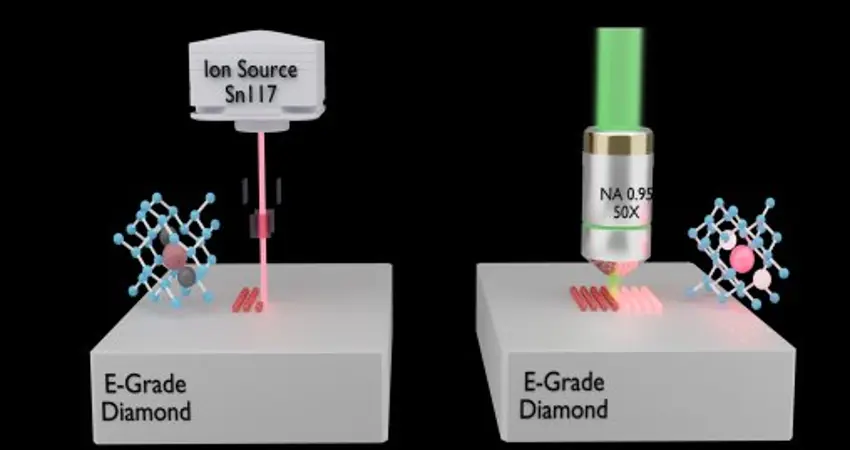
Schematic illustrating the process of ion implantation followed by femtosecond laser annealing
New research published in Nature Communications outlines an important step towards the scalable manufacture of nodes in future quantum optical networks.
The study was led by Oxford Professors Patrick Salter (Engineering Science) and Jason Smith (Materials), with contributions from former Oxford colleague Professor Dorian Gangloff, now at the University of Cambridge.
Colour centres are point defects in optically transparent materials which interact with light in unique ways, allowing them to emit single photons or exhibit quantum coherence properties. These colour centres, including ‘group-IV’ colour centres such as silicon-vacancy (SiV), germanium-vacancy (GeV), and tin-vacancy (SnV) centres in diamond, offer stable optical and spin properties which can be utilised as building blocks in quantum information technologies.
Traditionally, activating these colour centres required high-temperature annealing processes, which are not conducive to scalable manufacturing. Annealing is a treatment process that exposes the entire sample to extreme temperatures, to develop a refined structure.
The Oxford-led team developed a novel laser-based technique that enables the activation of individual colour centres at room temperature. The method involves using focused laser light to locally modify the diamond lattice, creating the desired colour centres with high spatial precision. Real-time monitoring of the fluorescence signal during the laser processing allowed the observation of dynamic processes involving the creation and destruction of other defect species, providing insight into the underlying science.
Professor of Photonic Materials and Devices, Jason Smith, in the Department of Materials at Oxford, says, “Our latest paper shows the power of laser processing combined with in-situ spectroscopy to engineer individual atomic scale defects in crystalline materials and to provide a new probe of the dynamics of defects during annealing. Observing these dynamics at the single defect level is critical to developing a clear understanding of the physical and chemical processes that occur within the material, which will in turn bring benefits to wide ranging applications in which point defects enhance or limit device function.”
This breakthrough has several significant implications:
- Scalability: The ability to activate colour centres with a laser allows for precise placement, essential for building large-scale quantum networks.
- Integration: The room-temperature process is compatible with existing semiconductor fabrication techniques, facilitating the integration of diamond-based qubits into current technologies.
- Performance: The laser-activated colour centres exhibit excellent optical properties, including high degrees of optical and spin coherence, critical for quantum communication and computing applications.
Professor Patrick Salter, Department of Engineering Science at Oxford explains, "Aside from the exciting prospects the work presents for quantum technology and the science of defect investigation, it also demonstrates a new standard of feedback for laser manufacturing, where the live spectroscopic information retrieved from the machining focus is critical for successful device fabrication."
The results are an important step towards the scalable manufacture of nodes in future quantum optical networks.


