20 May 2020
Bringing Order to Disorder in Liquid Crystals
Researchers at the Department of Engineering Science have found a new way to guide the topological defects of liquid crystals using lasers
In many branches of physics, ‘topological defects’ are critical for explaining the properties of materials; ranging from semiconductors to steel. Topological defects are points of disorder in an ordered system. For example, if a group of fish in a pond must follow each other head to tail then the fish will arrange themselves in concentric circles to follow the criteria. However, the fish at the centre has no other fish to follow and therefore no rule on which direction it must face (see image below). This illustrates a topological defect. It works this same way in liquid crystals if, instead of fish, you have liquid crystal molecules.
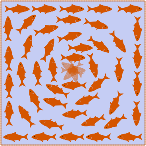
An illustration of a topological defect from lead author John Sandford O’Neill’s article explaining the concept behind the paper.
In liquid crystal displays (LCDs), found in TVs, monitors and phone screens, these defects have historically been considered a problem as they harm the performance and efficiency of the display. However, in recent years, researchers have increasingly seen defects as a useful technological and scientific tool, enabling new applications of liquid crystal materials.
In their new study, John Sandford O’Neill, Dr Patrick Salter, Prof Martin Booth, Prof Steve Elston and Prof Stephen Morris (from the Soft Matter Photonics and Dynamic Optics and Photonics research groups) use a femtosecond laser, one which emits incredibly short pulses of light, to create microscopic polymer structures inside liquid crystal devices. The process they use is known as direct laser writing. By writing these structures in different configurations they can precisely control and stabilise defects inside the liquid crystal. Sandford O’Neill explains, “In direct laser writing we use ultrafast lasers to initiate polymerisation in tiny volumes that are commonly referred to as “voxels” [a 3D version of a pixel]. By scanning the laser through the sample with sophisticated nanopositioning stages, we can fabricate a 3D polymer microstructure as if we were drawing it with a pen.”
In the past few years, research has shown that complex networks of topological defects can be used as microscopic templates that direct the self-assembly of nanomaterials, which are being explored for drug delivery applications. They have also found use in photonics and microscopy as a type of spatial light modulator able to shape light waves in unconventional ways to enhance the imaging quality of microscopes and telescopes.
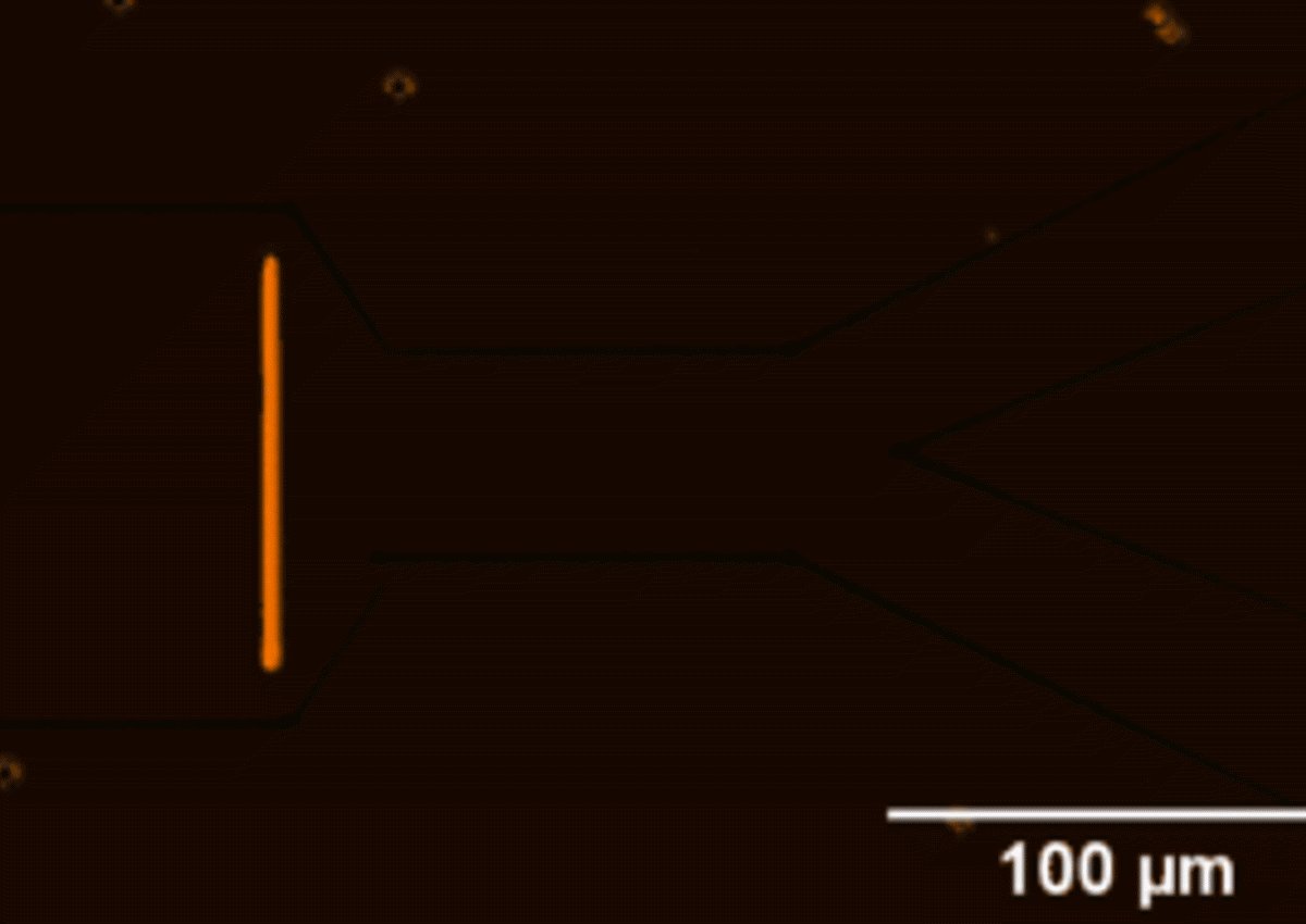
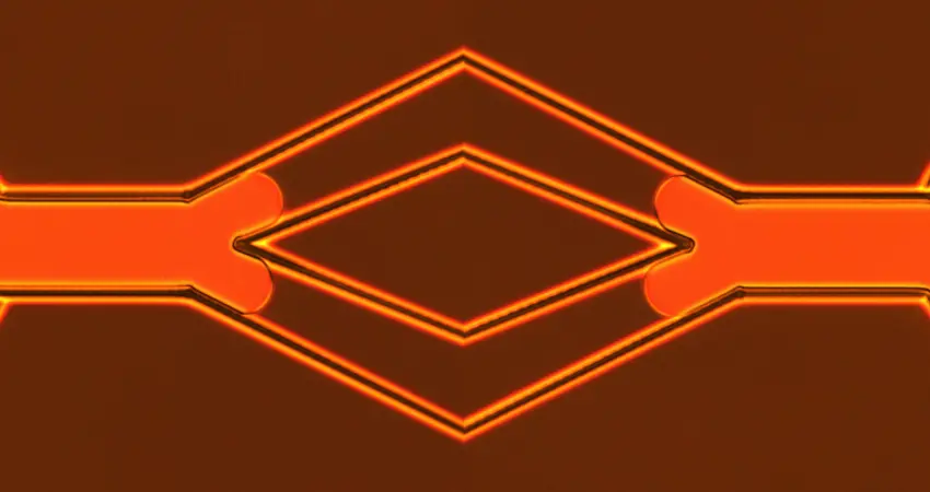
Defect confinement channels created with direct laser writing
This technique provides a powerful fabrication tool to researchers interested in topological defects from both a theoretical and practical perspective. John adds, “We hope that our paper will bring further attention to the fascinating area of topological defects and that our fabrication technique will enable future technological applications that go a step further in bringing order to disorder in liquid crystals”.
“Liquid crystals are truly fascinating materials with emerging applications in many areas beyond LCDs. We’ve shown how topological defects can now be controlled and engineered, opening the door to innovative new applications using defects to manipulate nanomaterials and light itself”
The paper is open access and is named “Electrically-tunable positioning of topological defects in liquid crystals”. Further explanation of the technology can be found in a “behind the paper” article by lead author John Sandford O’Neill.